Flexibility in PCB Fabrication
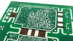
PCB Fabrication
Unlike rigid PCBs, flexible circuit boards are designed to bend and curve. They are typically manufactured using reel-to-reel technology to minimize manual handling. This process allows flex circuits to be more complex. In addition, a flex circuit can be designed to fit into narrow spaces where rigid PCBs can’t. This is especially useful in consumer electronics products such as wrist-watches.
When designing a flex circuit, it’s important to decide how much bending will be required. For example, if the flex-circuit section will remain static and not bend repeatedly – such as in an ultrasound device – you’ll be able to choose a higher number of layers, thinner copper thicknesses, and other design parameters. Conversely, if your flex-circuit section will undergo repeated bending and folding – such as in a portable computer – you should be careful to minimize stress concentration points by minimizing the number of folds and limiting the length of the flex-circuit section.
The choice of materials is also critical for a flex-circuit’s success. Professionals recommend a copper-clad laminate (CCL) with polyimide film because it offers exceptional thermal control, preventing softening or melting. It is also elastic and resilient, which increases a flex-circuit’s lifespan. In addition, a CCL with polyimide film provides excellent electrical insulation.
Flexibility in PCB Fabrication
Other crucial considerations for a flex pcb fabrication include the design of the traces and their routing. For instance, the flex-circuit’s bending radius should be large enough to avoid sharp angles that shorten its lifespan. Conductor traces should also be routed perpendicular to the general bend. In a flex-circuit with two or more layers, staggering traces on the top and bottom will eliminate I-beaming that thins out trace copper. Additionally, a gradual change in trace width is preferable to sharp changes.
Drill-to-copper distances are also an important factor to consider for a flex circuit. Vias that are too close to the flex material are susceptible to cracking or peeling. In addition, excessive stress at the via-copper connection can cause a broken solder joint. In order to prevent this from happening, it’s a good idea to use teardrop or pad fillet-shaped vias to connect plated through holes and traces in your flex circuit. This will help to reduce stress concentration and increase reliability.
In addition, flex-circuit designers should use anchoring stubs to ensure proper component mounting on the flex circuit. To do this, the stubs should be anchored with plating and have reduced coverlay access openings. This will eliminate the need for splices.
Finally, a flex-circuit’s thickness is another key factor in its cost. A high layer count adds complexity to the lamination process, resulting in higher production costs. This can be mitigated by reducing the number of layers, selecting the correct copper thickness, and using panel utilization strategies to maximize material utilization. Lastly, designers should pay attention to the selection of surface finishes and plating options, which will also impact costs. For instance, dual-surface finishing requires additional labor and materials and is generally more expensive than single-surface finishing.